
Precision is the defining characteristic of semiconductor manufacturing, especially as the industry pushes toward 3nm nodes, and as AI chip demand continues to place extraordinary pressure on fab output.
Because of this the margin for error at the inspection stage has never been smaller, where, after 1,000 process steps, a 99.5% yield can mean that less than 1% of devices function flawlessly.
It’s uncomfortable arithmetic, one that keeps many process engineers awake. And it is why the choice of visual inspection tooling, often treated as a secondary concern, may deserve more attention than it typically gets.
In fact, according to Grand View Research, the global semiconductor inspection equipment market in 2024 was valued at USD 5.6 billion, and is projected to nearly double to USD 12.15 billion by 2033, driven precisely by this intensifying demand.
Within that growth, optical inspection for a third of that growth owing to its accessibility and workflow compatibility for majority of the inspection tasks that happen outside the automated wafer scanner, be it on the production flow, in the QC lab and in the failure analysis suite. And this is where digital microscopy earns its place
Main Areas of Application
Not every inspection task is the same, and equipping a team as though it were is a common and costly mistake. In practice, semiconductor visual inspection operates across two distinct modes: rapid in-line checks that need to keep pace with production throughput, and deep dive analysis sessions where engineers need to characterise a defect fully before making a process decision.
Trying to serve both purposes with a single general purpose tool usually means compromising one or the other, slow throughput during production checks or insufficient detail during root cause analysis. The smarter approach is to match the tool to the task.
The Leica Empira 3 is designed for in-line or at line quality control at the macro and mesoscale, while the Leica DVM6 is designed for in-depth failure analysis at the meso and microscale. Together they form a complementary pair.
Leica Emspira 3: Inspection that Keeps Pace with Production
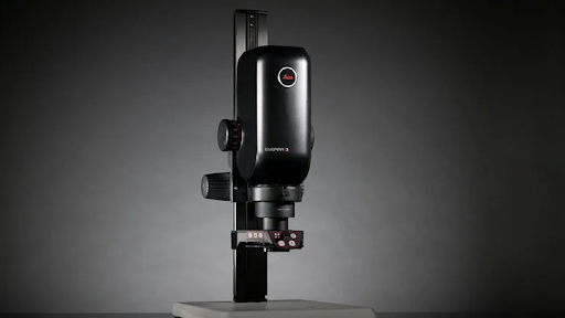
The Emspira 3 is built around a simple premise: inspectors should spend their time inspecting, not managing a workstation. It operates in stand-alone mode with an on-screen display, allowing teams to measure, annotate, and share results without a PC — eliminating the need to move between workstations for different steps in the process.
For a semiconductor production environment where throughput targets are non-negotiable, this matters. The quick start time, fast zooming, and 4K live image at up to 60 frames per second mean that little or no waiting time is introduced into the inspection workflow. The absence of eyepieces is also a practical ergonomic gain on a busy floor — engineers can work in a natural posture and share the live image on-screen during team reviews without having to rotate the instrument
Pass/fail decisions are supported by built-in comparison tools that allow operators to check live images directly against reference images or customised overlays in a single click. User roles can be configured to protect the system from unwanted changes in regulated production environments, which is particularly relevant in contexts where process integrity must be maintained across shifts and operators.
The Emspira 3 is powered by the Enersight software platform, which brings measurement, documentation, and sharing into one interface — whether connected to a network or working offline. For teams managing documentation requirements or ISO-aligned quality systems, the ability to push images directly to a network without USB transfer is a meaningful efficiency gain.=
Leica DVM6: From the Production Floor to the Root Cause

Where the Emspira 3 answers the question “Is this component within specification?”, the DVM6 is built to answer the harder question: “Why isn’t it?”
The DVM6 features a 10-megapixel high-resolution camera with fast live image display, Leica PlanApo-corrected optics, and a 16:1 zoom range that allows operators to move seamlessly from an overview of the component down to fine structural detail without losing focus or needing to re-adjust.
The tilting function allows observation of samples from -60° to +60°, enabling inspection of hard-to-image regions that would be invisible from a standard top-down view. For semiconductor failure analysis — where a solder joint crack, delamination, or surface contaminant may only be visible from a specific angle — this is not a cosmetic feature; it is fundamental to the work.
Measurement accuracy is among the lowest uncertainty available in digital microscopy, with repeatability on the XY-axis of ±3µm and Z-axis of ±0.5µm. All instrument components are sensor-encoded, meaning settings are saved with every image, and results are reproducible regardless of which operator performed the inspection. For R&D environments where data integrity underpins process decisions, that reproducibility is critical.
The DVM6’s LAS X software supports both 2D and 3D analysis, with reporting templates that allow engineers to generate structured documentation directly from their investigation — reducing the time from observation to corrective action.
Choosing the Right Tool for Your Workflow
The question for most semiconductor engineering teams is not whether to invest in digital microscopy — it is where in the workflow that investment delivers the highest return.
For teams that need faster, more consistent decisions on the production line, the Emspira 3 brings lab-grade imaging to the floor without the lab-grade setup overhead. For engineering teams working on failure analysis, process development, or incoming component qualification, the DVM6 provides the optical performance and analytical depth to characterise defects conclusively.
For operations that span both needs — and most do — running both systems in tandem means a defect identified on the line can be escalated immediately to the engineering lab for analysis, with a documented image trail from detection to root cause.
Gennex supplies both the Leica Emspira 3 and the Leica DVM6 as part of its semiconductor solutions portfolio. To discuss which configuration suits your inspection requirements, contact the Gennex team.