
Semiconductor Assembly
High-Precision Semiconductor Assembly for Reliable Performance
At Gennex, semiconductor assembly services transform silicon dies into fully functional, production-ready components. With a focus on precision, scalability, and reliability, we support advanced packaging and high-volume manufacturing across a wide range of industries. From initial die attach to final testing, every step of our semiconductor assembly process is optimized to ensure consistent quality and long-term performance.
What is Semiconductor Assembly?
Semiconductor Assembly, often referred to as the back-end process—follows wafer fabrication and involves singulating chips, attaching them to substrates, creating electrical interconnections, and encapsulating them for protection. This process:
Converts fragile silicon dies into robust, usable components
Enables electrical connectivity to PCBs and systems
Provides thermal management and mechanical protection
Supports advanced architectures like 3D integration and chip stacking
Our Semiconductor Assembly Capabilities
-
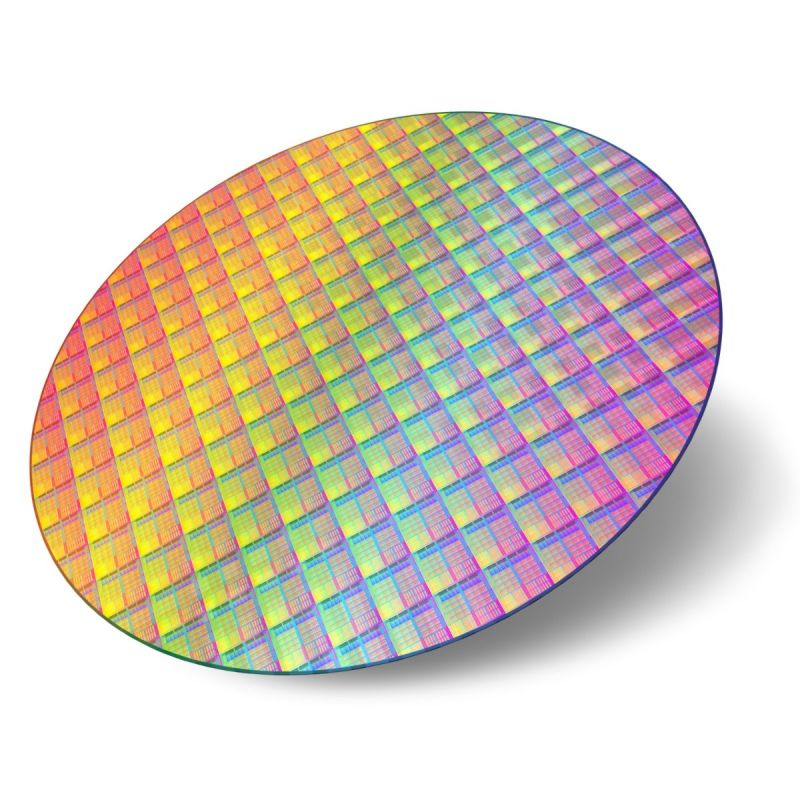
Custom Wafer
-
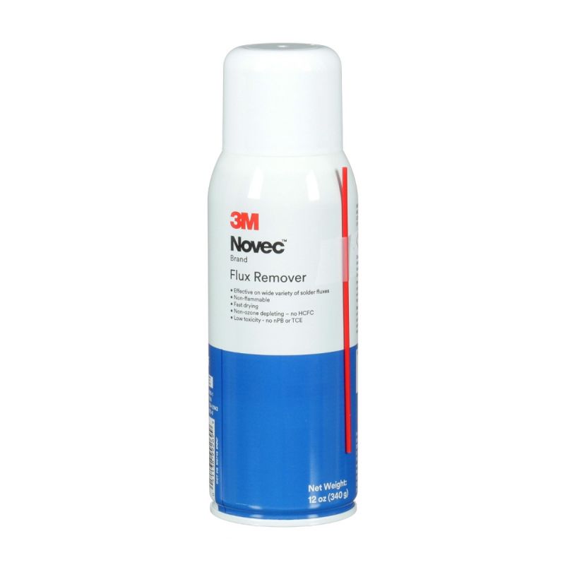
Novec Flux Remover
-
Patterned Wafer
-

Novec Electronic Degreaser
-

Aluminized Wafer
-

Novec Contact Cleaner
-
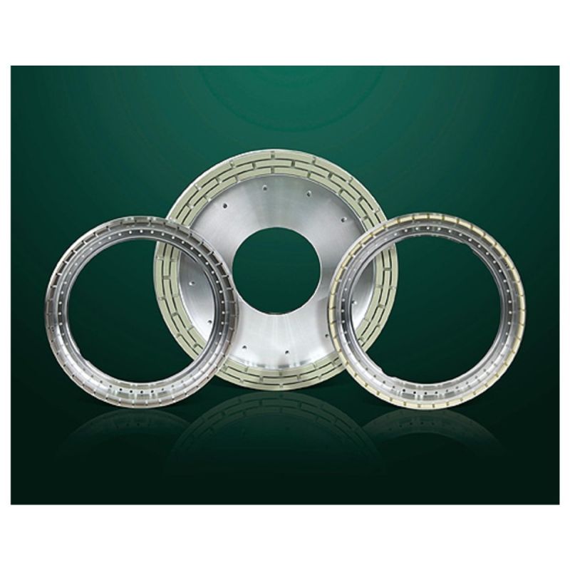
Back Grinding Wheel
-
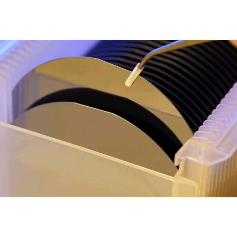
Silicon Wafer
-
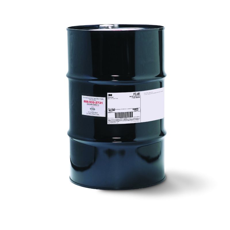
Fluorinert - Thermal Management
-
Porous Ceramic Chuck Table
-
Carrier Tapes
-
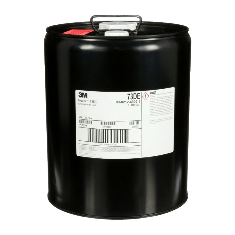
Novec Engineered Fluid
-
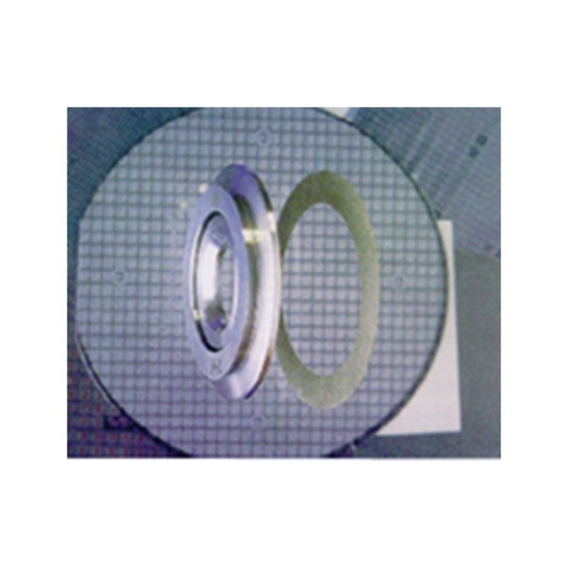
Wafer Dicing Blade Flange
Semiconductor Assembly Process Overview
Gennex streamlined semiconductor assembly process is designed for efficiency, precision, and high yield:
Wafer Dicing – Separating individual semiconductor dies
Die Attach – Secure placement onto substrates
Interconnection – Wire bonding or flip-chip attachment
Encapsulation – Protecting the device from external factors
Testing & Inspection – Verifying functionality and durability
Final Packaging – Preparing units for integration and shipment

Industries That Rely on Semiconductor Assembly
Our semiconductor assembly services are trusted across multiple sectors:
Consumer Electronics
Automotive and EV Systems
Telecommunications and 5G Infrastructure
Industrial Automation
Medical and Healthcare Devices
Why Choose Gennex for Semiconductor Assembly Services?
Whether it requires standard packaging or advanced integration solutions, Gennex deliver reliable semiconductor assembly services tailored to your product requirements.
- High Precision & Reliability
We utilize advanced equipment and automation to achieve micron-level accuracy and consistent output. - Scalable Manufacturing
From prototyping to high-volume production, our processes are optimized for scalability and efficiency. - Advanced Technology Integration
We support next-generation packaging and integration techniques to meet evolving industry demands. - Quality-Driven Approach
Every stage of our assembly process is governed by strict quality control protocols to ensure long-term reliability.
Get in touch with our team today to discuss your project and discover how we can support your semiconductor manufacturing needs. Email contact@gennexcorp.com for your tailored solutions.
Frequently Asked Questions for Semiconductor Assembly
Semiconductor assembly is the back‑end process that takes individual silicon dies and integrates them into protective packages with electrical connections, making them ready for use in electronic systems. It’s essential for mechanical protection, thermal management, and enabling reliable connections to circuit boards or systems. Gennex offers comprehensive assembly services that ensure your chips are packaged reliably for robust field performance.
Typical assembly flows include die attach (mounting the die to a substrate or lead frame), wire bonding or flip‑chip interconnect to provide electrical paths, encapsulation/molding for protection, testing and inspection, and final marking and packing. Gennex can support these key steps with end‑to‑end assembly solutions customized to your design needs. For further inquiries, email contact@gennexcorp.com.
Wire bonding connects the die to the package with fine wires, usually gold or aluminum, and is widely used due to maturity and cost‑effectiveness, while flip‑chip assembly places solder bumps on the die and bonds it face‑down to the substrate for shorter electrical paths and better thermal performance. Gennex works with both technologies and can recommend the best interconnect method for your application — email contact@gennexcorp.com.
Proper assembly ensures electrical integrity, thermal dissipation, and mechanical protection. Poor bond quality, misalignment, or inadequate encapsulation can lead to failures in the field, so rigorous control of assembly processes improves yield and long‑term reliability. Gennex provides quality‑driven assembly processes that help minimize defects and maximize device performance.
To begin, you’ll typically provide your die or wafer specifications, desired package type, volume projections, and performance requirements so an appropriate assembly plan can be recommended. Gennex can review your information and propose a customized assembly solution that fits both technical goals and production timelines. — email contact@gennexcorp.com to check lead times for your project. Bookmarksgrove right at the coast