Plastronics

Plastronics Test Sockets for Semiconductor Test
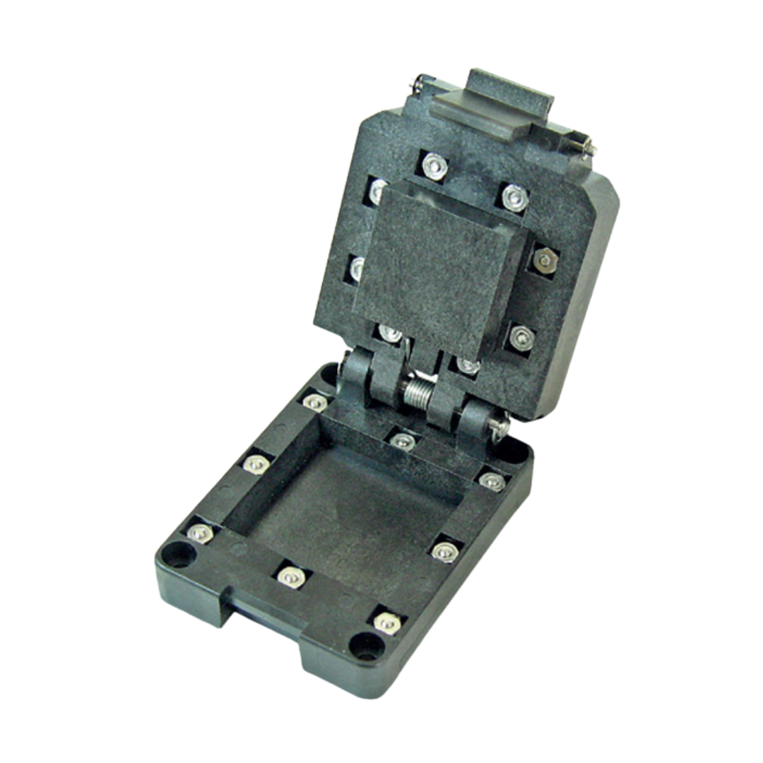
Plastronics provides advanced IC test socket solutions engineered for high-performance semiconductor testing applications. Designed to support demanding environments such as high-frequency, high-current, and high-temperature testing, these solutions deliver reliable electrical performance, durability, and consistent contact integrity for various package types and testing requirements.



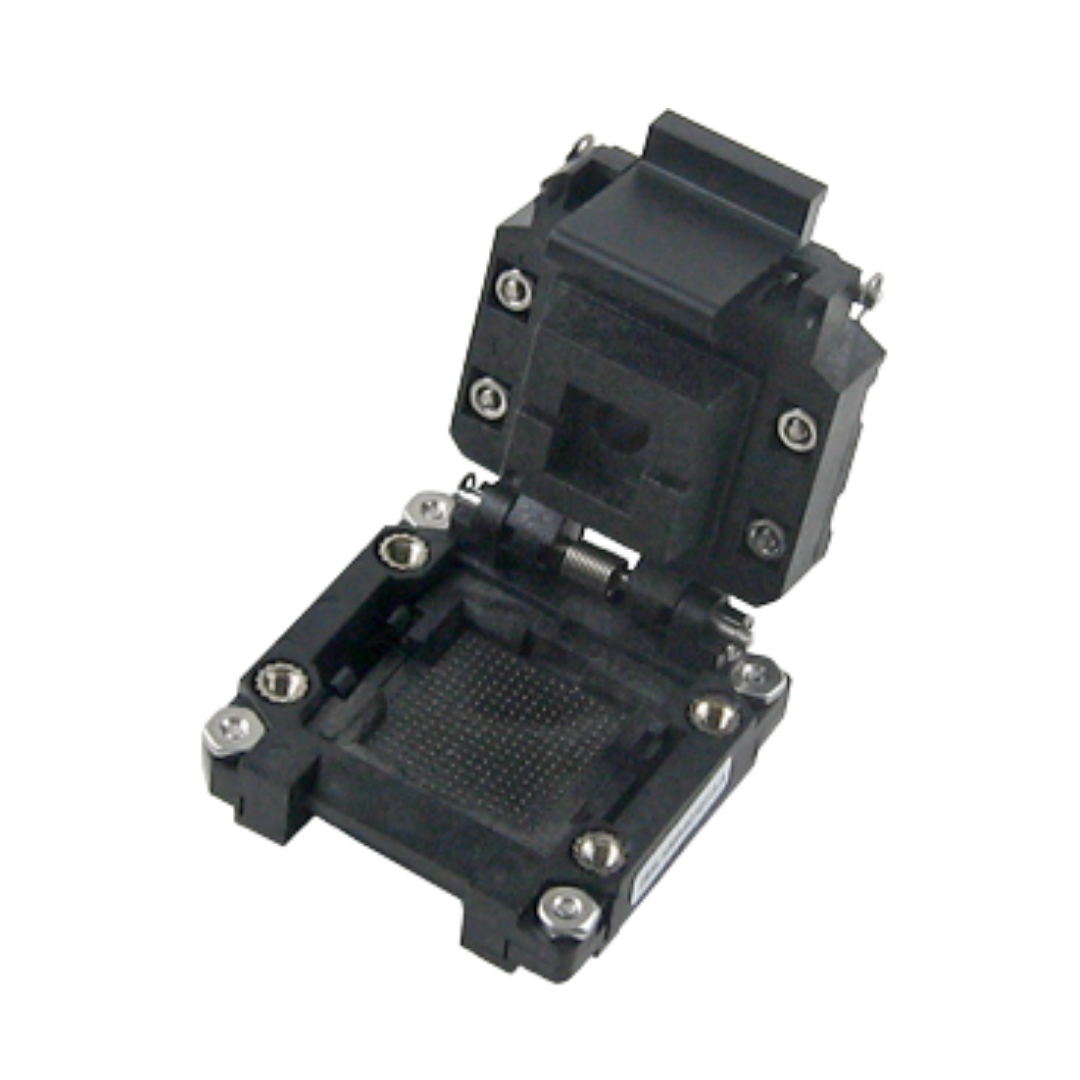
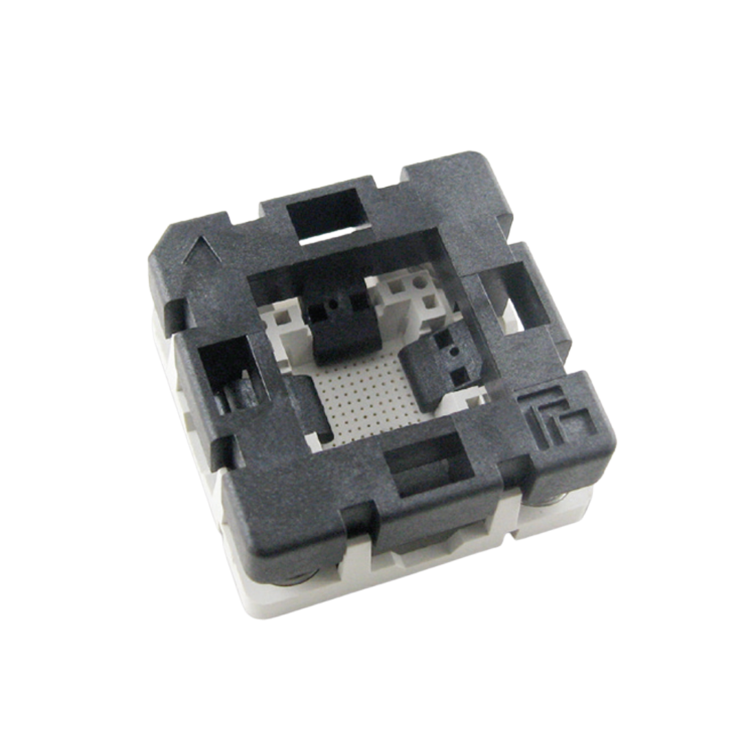

Features & Advantages of Using Plastronics Solutions
Plastronics test sockets are engineered to meet the growing demands of modern semiconductor testing. By combining innovative contact technology with durable construction, these solutions help improve test reliability, electrical performance, and long-term operational efficiency.
Key Features:
- High Reliability Performance – Maintains stable electrical contact during repeated testing cycles.
- Excellent Signal Integrity – Supports high-speed and high-frequency semiconductor testing applications.
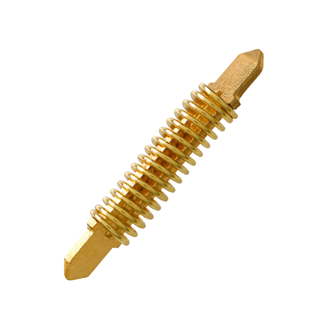
- Durable H-Pin® Technology – Designed for extended operational life and consistent performance.
- Wide Device Compatibility – Supports various semiconductor package types and testing requirements.
- Optimized Thermal Performance – Performs reliably in high-temperature and thermal cycling environments.
- Precision Contact Design – Helps improve testing consistency and reduce contact-related issues.
Plastronics H-Pin® Socket Series
-
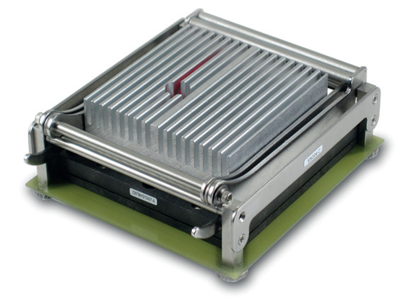
ES Series H-Pin® Socket
-

Q-Series H-Pin® Socket
-
K Series H-Pin® Socket
-

R-Series H-Pin® Socket
-
M-Series H-Pin® Socket
-

H-Pin®
-

C-Series H-Pin® Socket
-

D Series H-Pin® Socket
Benefits of Plastronics Semiconductor Test
Choosing the right semiconductor test socket plays an important role in improving testing performance and reducing operational challenges. Plastronics solutions are designed to help semiconductor manufacturers achieve more efficient and reliable testing processes.
Key Benefits:
- Improved Test Accuracy – Helps reduce signal inconsistencies and testing errors.
- Increased Operational Efficiency – Durable construction minimizes maintenance requirements and downtime.
- Enhanced Product Reliability – Supports consistent semiconductor validation results.
- Flexible Integration – Compatible with various semiconductor testing systems.
- Longer Service Life – Designed to withstand repeated insertion cycles and demanding environments.
- Reduced Testing Interruptions – Maintains dependable electrical contact during operation.

Right Plastronics Solution for Your Application
Plastronics socket solutions are widely used across semiconductor manufacturing and testing environments where accuracy, durability, and reliable electrical performance are essential. These solutions support a broad range of applications for both engineering and production testing processes.
Typical Applications:
- High-frequency semiconductor testing
- Burn-in and reliability testing
- Engineering evaluation and validation
- Production IC testing
- Automotive semiconductor testing
- RF and high-speed device testing
- Advanced package validation
- Semiconductor research and development
Need Plastronics Solution for Your Project?
Selecting the appropriate test socket solution is essential for achieving accurate and efficient semiconductor testing results. Our team can help identify the right Plastronics products based on your device package, testing requirements, and operational conditions.
Support Services:
- Product consultation
- Technical assistance
- Socket selection guidance
- Semiconductor testing support
- Product inquiries and quotations
Contact us today to learn more about available Plastronics solutions and discover the right semiconductor testing products for your application requirements. Email semicon.rfq@gennexcorp.com for your tailored solutions.
Frequently Asked Questions for Plastronics
Plastronics H-Pin® test sockets are designed for semiconductor testing applications including final test, burn-in, characterization, reliability testing, and high-frequency IC validation. These sockets are commonly used for testing BGA, QFN, LGA, WLCSP, and other advanced semiconductor packages in automated test environments. Gennex can help you identify the right Plastronics socket configuration for your semiconductor testing requirements — email semicon.rfq@gennexcorp.com for technical assistance.
Plastronics sockets support a wide range of semiconductor package types including BGA, QFN, LGA, CSP, WLCSP, SIP, and custom IC package formats. Different socket series are optimized based on pitch, thermal requirements, electrical performance, and handler compatibility. Gennex can help recommend the ideal Plastronics socket solution for your device package and testing process — email semicon.rfq@gennexcorp.com for application support.
H-Pin® socket technology provides excellent electrical performance, low inductance, high durability, stable contact resistance, and reliable signal integrity during semiconductor testing. It is particularly suitable for high-frequency, high-speed, and fine-pitch IC applications. Gennex can help evaluate whether H-Pin® technology is suitable for your semiconductor test requirements — email semicon.rfq@gennexcorp.com for consultation.
Each Plastronics H-Pin® socket series is designed for specific semiconductor testing requirements such as package compatibility, pitch size, electrical performance, thermal capability, and mechanical durability. The correct series selection depends on the IC package type, test environment, and production setup. Gennex can help you compare Plastronics socket series and recommend the most suitable option for your application — email semicon.rfq@gennexcorp.com for assistance.
Yes, Gennex provides technical assistance, product recommendations, and sourcing support for Plastronics semiconductor test sockets across Southeast Asia and other supported regions. Our team works closely with semiconductor manufacturers, OSAT companies, and electronics firms to help address semiconductor test challenges. Gennex can support your semiconductor test socket requirements and application needs — email semicon.rfq@gennexcorp.com to connect with our team.