Die Prep
Precision Die Prep for High-Yield Semiconductor Assembly
At Gennex, Die Prep for semiconductor assembly ensures that every wafer is accurately processed into high-quality individual dies, ready for packaging and integration. With advanced equipment and tightly controlled processes, we minimize defects, improve yield, and prepare each die for reliable downstream semiconductor assembly. From wafer thinning to die picking, our die preparation solutions are built to support modern, high-performance semiconductor applications.
What is Die Preparation (Die Prep)?
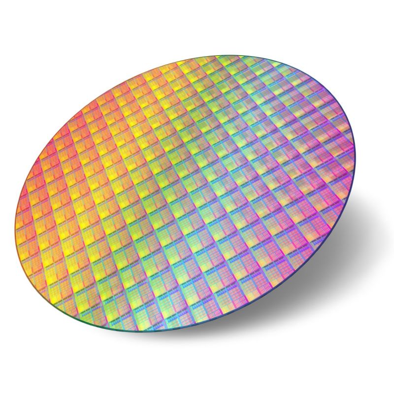
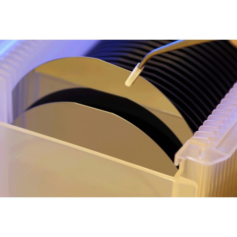
Die Preparation or Die Prep in Semiconductor Assembly is the process of preparing semiconductor wafers for packaging by separating them into individual dies and ensuring they are ready for attachment and interconnection.
This stage typically includes wafer mounting and dicing, where wafers are securely mounted on tape and then cut into individual chips for further processing.
As a critical step in semiconductor assembly, die prep directly impacts:
Device yield and performance
Mechanical integrity of each die
Cleanliness and contamination control
Efficiency of downstream assembly processes
Our Die Prep Capabilities for Assembly
Die Prep Process for Semiconductor Assembly
Gennex Die Prep process is optimized for precision, consistency, and high throughput:
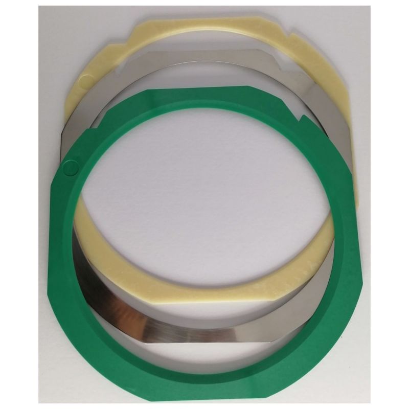
Wafer Mounting – Attaching wafers to frames with adhesive tape
Wafer Thinning – Reducing thickness for advanced packaging
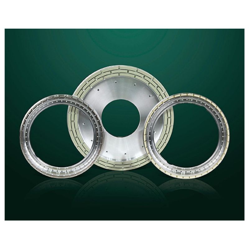
Wafer Dicing – Cutting wafers into individual semiconductor dies
UV Treatment & Tape Expansion – Facilitating clean die separation
Die Inspection – Identifying defects and ensuring quality
Pick & Place – Preparing dies for the next stage of semiconductor assembly
This process ensures that each die is structurally sound and ready for high-reliability semiconductor assembly applications.
Applications of Die Preparation (Die Prep)
Our die prep for semiconductor assembly supports a wide range of applications requiring precision and reliability:
Consumer Electronics – Enables compact, high-performance chips for smartphones, laptops, and wearable devices.
Automotive & Power Devices – Supports semiconductor assembly for sensors, control units, and power management systems with durability and thermal efficiency.
Telecommunications & 5G – Prepares high-frequency semiconductor devices for networking and communication infrastructure.
Industrial & Automation Systems – Ensures robust die preparation for control systems, robotics, and smart manufacturing technologies.
Medical Electronics – Provides high-quality die prep for semiconductor assembly used in diagnostic and life-critical devices.
Why Choose Gennex to Support Your Die Prep Needs?
We provide end-to-end die prep solutions for semiconductor assembly, ensuring that every die is accurately prepared for packaging and integration.
- Improved Yield and Reliability
Precision die prep minimizes breakage, contamination, and defects—ensuring better outcomes in semiconductor assembly. - Advanced Process Control
We use tightly controlled parameters to maintain consistency across every wafer and die. - Scalable Production
Our die prep solutions are designed to support both prototyping and high-volume semiconductor assembly. - Cleanroom Environment
All die preparation processes are performed in controlled environments to maintain the highest quality standards.
Contact us today to learn how our die prep expertise can enhance your semiconductor assembly process and improve overall product performance. Email semicon.rfq@gennexcorp.com for your tailored solutions.
Frequently Asked Questions for Die Prep
Key processes include wafer mounting, wafer thinning/backgrinding to reduce thickness, cleaning, precise wafer dicing to separate dies, and inspection and sorting of finished dies. Each step must be tightly controlled to protect fragile structures and maximize yield. Gennex can advise on optimal process selection and execution tailored to your specifications, semicon.rfq@gennexcorp.com now.
Thinning reduces wafer thickness to meet advanced packaging, size, weight, and thermal goals. It also makes dicing and downstream assembly more precise and reliable, helping avoid warpage or stress that can damage dies. For advanced thinning solutions and quality assurance, Gennex can guide you, email semicon.rfq@gennexcorp.com. Â
Common methods include mechanical blade dicing, laser dicing, stealth or plasma‑assisted dicing — each with strengths for different materials, die thicknesses, and precision requirements. Choice depends on wafer material, die layout, thickness, and acceptable risk of edge damage or contamination. Gennex can help you evaluate and select the best dicing approach for your needs, email semicon.rfq@gennexcorp.com to explore your options.
Challenges include die edge chipping, microcracks, burrs, particle contamination, and tape delamination during cutting. Proper maintenance and calibration of tools, choice of dicing tape, and integrated cleaning systems reduce defects and improve overall yield. For solutions that address these challenges, Gennex offers expert support and technology recommendations, email semicon.rfq@gennexcorp.com.
To begin, you’ll typically provide wafer specifications (material, diameter, thickness), target die size/layout, and any special handling or precision requirements so the best die prep plan can be recommended. Gennex can review your requirements and propose tailored die prep solutions, email semicon.rfq@gennexcorp.com to check lead times for your project. Bookmarksgrove right at the coast