
Singapore occupies a unique position in the global semiconductor supply chain. With nine of the world’s top 15 semiconductor companies operating locally and an industry valued at USD 70 billion in 2025, Singapore has developed a deeply integrated ecosystem spanning wafer fabrication, advanced packaging, and precision equipment manufacturing. Within that ecosystem, PCB assembly plays a role that is easy to underestimate and costly to get wrong.
Semiconductor applications place demands on PCB assembly that general electronics manufacturing does not. The boards that support burn-in testing, reliability assessment, process control, and semiconductor test infrastructure must be assembled to a level of precision and material consistency that standard commercial assembly cannot guarantee.
Finding a PCB assembly partner in Singapore with the specific capability to meet those demands, and the service breadth to support the full production workflow, is a different exercise from sourcing a commodity PCB assembler.
At Gennex, we provide PCB assembly in Singapore across the full scope of what semiconductor applications require, from initial design through fabrication, assembly, specialist board production, and repair.
PCB Design Services
The quality of a PCB assembly begins long before components are placed. Design decisions, whether it’s layer stackup, material specification, trace geometry, determine how a board performs under the conditions it will actually face in a semiconductor environment. Catching design issues at this stage is substantially less expensive than resolving them after fabrication.
Our PCB design services support teams from schematic through to production-ready Gerber files, with design-for-manufacturability consultation built into the process. For teams working on new product introductions or engineering revisions, our quick-turn prototyping capability allows design iterations to be validated rapidly before volume production is committed.
PCB Fabrication
Fabrication quality is the foundation on which assembly performance is built. Material selection, copper weight, layer registration, and surface finish are fabrication variables that directly affect how a board performs in service, particularly in semiconductor applications where thermal cycling, sustained electrical load, and signal integrity requirements are more demanding than in standard commercial electronics.
Our PCB fabrication capability covers the range of substrates and specifications that semiconductor applications demand, from standard FR-4 for lower-stress applications to high-Tg materials for boards that must withstand elevated operating temperatures.
PCB Assembly
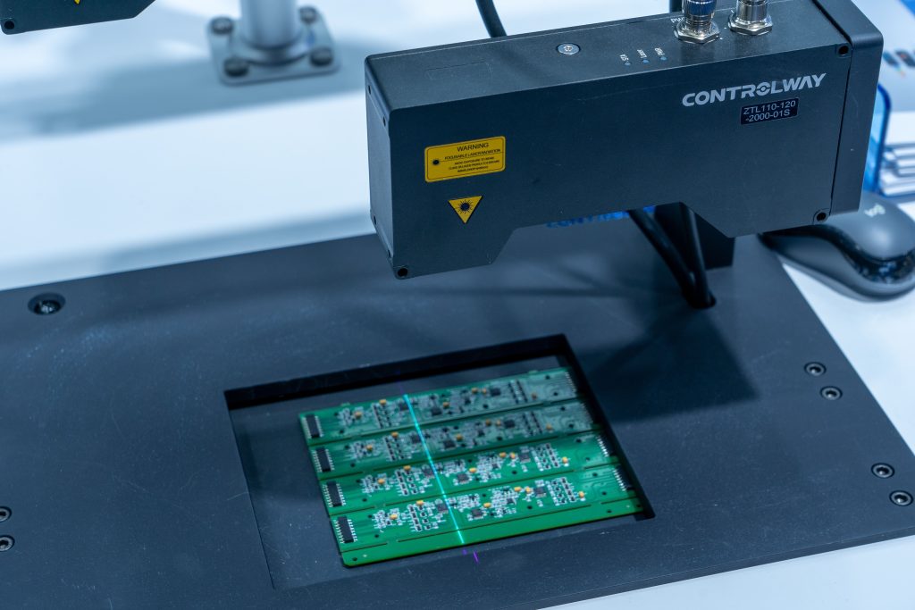
Component placement, soldering quality, and inspection discipline are the variables that determine whether a fabricated board performs to specification in service or introduces the kind of subtle, difficult-to-diagnose variability that affects test results and production throughput.
Compliance with IPC standards, ensures high-quality PCBs across fabrication and inspection criteria. Our assembly process incorporates quality control at each production stage, with inspection documentation that provides the traceability semiconductor customers require. For teams managing quality systems subject to audit, this documentation discipline is a baseline requirement rather than a value-added feature.
Our prototyping and quick-turn assembly capability supports teams at the development stage, where speed of iteration matters as much as production quality. Schematic and BOM-provided design-to-PCBA services allow customers to move from design intent to assembled board without managing multiple supplier relationships across the design and assembly stages.
Specialist Semiconductor Boards
The most distinctive dimension of our PCB assembly capability in Singapore is the range of specialist board types we support, boards designed specifically for semiconductor test and reliability applications that general PCB assemblers typically cannot produce to the required standard.
Burn-in boards and burn-in sockets carry semiconductor devices through sustained high-temperature, high-voltage stress testing designed to screen for early-life failures. These boards must operate at extreme heat levels, requiring materials with higher glass transition temperature values and broader trace widths to carry the higher currents of electrical load testing. Assembly precision and material specification at this level are non-negotiable, a board that fails during burn-in invalidates the test results it was assembled to produce.
Test During Burn-in (TDBI) boards add active electrical measurement to the burn-in process, allowing devices to be characterised under stress rather than only after the cycle completes. HAST boards are designed for highly accelerated stress testing under simultaneous elevated temperature and humidity, among the most demanding conditions any PCB assembly must withstand. Humidity test boards and life test boards support reliability qualification programmes that must demonstrate device performance over simulated operational lifetimes.
Systems driver boards and burn-in board backplanes form the infrastructure layer of the test system, distributing signals and power to the boards under test. Assembly quality at this level determines the consistency of what every device in the test run actually experiences.
Interface boards sit at the electrical boundary between the automated test equipment and the device under test, where every assembly variable in the signal path (pad geometry, via quality, surface finish) affects measurement accuracy.
ESA-Certified PCBs
For applications requiring compliance with European Space Agency standards, we produce ESA-certified PCBs to the stringent workmanship and traceability requirements that space and high-reliability applications demand. ESA certification represents one of the most demanding quality frameworks applied to PCB assembly, providing assurance that extends well beyond standard commercial or industrial certification.
PCB Repair
PCB repair capability is often overlooked in supplier evaluation but becomes practically important quickly. Burn-in boards and test boards operate under sustained stress and degrade over time. Our PCB repair services allow customers to manage their board inventory over its full operational life, extending the usable life of specialist boards and reducing the replacement costs that accumulate across multi-year semiconductor test programmes.
End-to-End PCB Assembly in Singapore
The value of our PCB assembly offering in Singapore is not in any single service. It is in the ability to manage the complete PCB workflow, from design consultation through fabrication, assembly, specialist board production, and repair, through a single partner with the semiconductor-specific experience to do each stage well.
For semiconductor teams in Singapore and across Southeast Asia, that consolidation reduces the complexity of managing multiple supplier relationships, maintains quality and documentation consistency across the production workflow, and provides a single point of accountability when performance questions arise.
We operate across Singapore, Malaysia, Thailand, and the Philippines, supporting PCB assembly requirements across the region’s most active semiconductor manufacturing markets. Get in touch with our team to discuss your PCB assembly requirements.