ESA Certified PCBs
PCB Testing Explained: From Burn-In Boards to ESA Standards
Discover how these burn-in boards, designed to stress test components, align with European Space Agency (ESA) standards to guarantee the highest quality. By grasping these concepts, you gain insight into the essential practices that safeguard the functionality of electronic devices across various applications, from consumer electronics to advanced aerospace systems.
Understanding PCB Testing
In-Circuit Test (ICT)
In-Circuit Test (ICT) checks individual PCB components using electrical probes, detecting defects like shorts, opens, and soldering errors to ensure proper function before advanced testing.
Functional Circuit Test
This simulates the environment in which the PCB will operate, assessing how the entire assembly behaves when subjected to typical operating conditions. By verifying the board’s functional performance, this test ensures that the PCB meets the expected design specifications and operates reliably within its intended application.
Design for Testing (DFT)
Incorporating Design for Testing (DFT) principles into PCB design streamlines the testing process by optimizing the board layout for both ICT and Functional Testing. By proactively designing PCBs with testing in mind, you minimize testing complexities and improve the efficiency and accuracy of the testing process.
Boundary Scan Testing
Boundary Scan Testing is an advanced technique used to assess connections between integrated circuits on PCBs. This method employs a standardized test protocol, enabling the identification of connection issues without requiring physical probe access to every test point.
Understanding Burn-In Testing
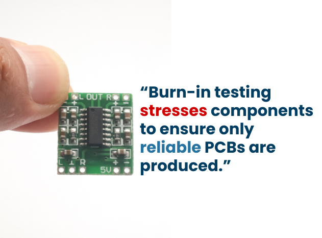
The primary aim of burn-in testing is to force components into failure or near-failure states, uncovering vulnerabilities that could compromise the overall reliability of the electronics.
By revealing these weaknesses early, manufacturers can ensure that only the most robust PCBs move forward in the production line.
Role of Burn-In Boards
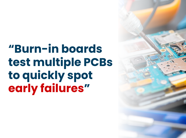
These specialized boards are engineered to house multiple PCBs during the burn-in testing phase, facilitating the simultaneous evaluation of numerous units.
By using burn-in boards, manufacturers can efficiently detect early failures across a batch of components, thus ensuring the quality and reliability of each individual PCB.
Importance for Product Reliability
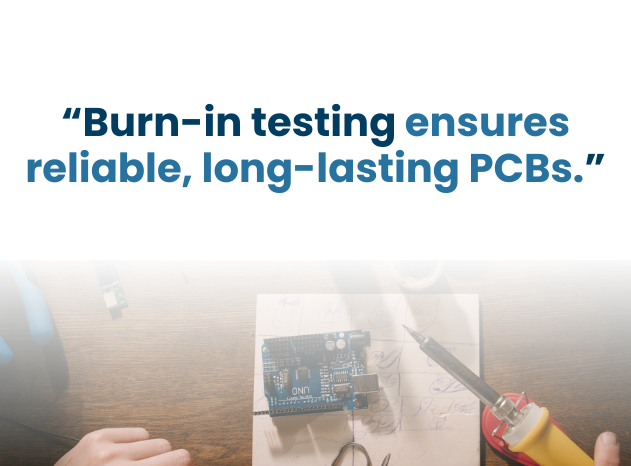
The significance of burn-in testing cannot be understated when considering product reliability. By exposing PCBs to harsh conditions, manufacturers can significantly lower failure rates, translating to higher customer satisfaction and reduced warranty costs.
This proactive approach to testing helps in preemptively identifying potential issues that could arise in the field, thereby extending the life expectancy of the final product.
The Importance of ECSS Standards
The Importance of ECSS Standards
When it comes to PCB testing within the European Space Agency (ESA) framework, the ECSS-Q-ST-70-60C standards are crucial.
These standards are developed by the European Cooperation for Space Standardization (ECSS) and ensure that PCB manufacturers meet the stringent requirements needed for space applications. Their purpose is to guarantee that printed circuit boards are reliable and capable of withstanding the harsh conditions encountered in space.
How ESA Qualification Impacts PCB Testing
The ESA qualification process for PCB manufacturers involves a rigorous assessment against ECSS standards. The testing protocols are designed to verify the reliability, durability, and performance of PCBs under extreme conditions such as temperature fluctuations, radiation exposure, and vacuum environments.
Incorporating ESA standards into PCB testing allows for a systematic evaluation of materials, design, and manufacturing processes.
Ensuring Signal Integrity and Impedance Control
PCB testing plays a critical role in ensuring these key attributes. Signal integrity involves the preservation of signal quality across PCB pathways, which is vital for preventing data errors and maintaining efficient communication.
By leveraging advanced PCB testing techniques, engineers can identify potential disruptions and address them proactively, thereby ensuring seamless transmission.
Impedance control, on the other hand, refers to the management of resistance in PCB circuits to ensure consistent electrical performance.
Through meticulous testing, one can verify that the impedance levels align with the designed specifications, minimizing signal loss and enhancing overall device reliability.
Power Delivery Optimization in Diverse Applications
PCB testing extends beyond the realm of signal integrity to encompass effective power delivery. This involves evaluating the power distribution network within the board to ensure it can handle the required load without overheating or causing energy inefficiencies. In a variety of applications, from consumer electronics to sophisticated industrial machinery, ensuring efficient power delivery is essential for operational durability and performance consistency.
Role of PCB Testing in the Medical Device Industry
In the medical device industry, the reliability of PCBs is of utmost importance. PCB testing ensures that medical devices operate safely, effectively, and without malfunction. Given the critical nature of these tools, from monitoring systems to diagnostic equipment, rigorous PCB testing is indispensable. It not only maintains the integrity of the devices but also upholds the trust placed in medical technology.
Looking for more than just PCB solutions?
At Gennex, we provide a complete range of semiconductor solutions—from reliable PCB testing and burn-in boards to advanced components for aerospace, automotive, and industrial applications. Our expertise ensures your electronics meet the highest standards of quality and performance.
Talk to our tech experts: contact@gennexcorp.com