
Key Features of Kepler Test Socket
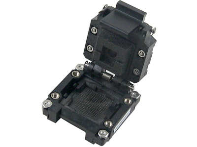
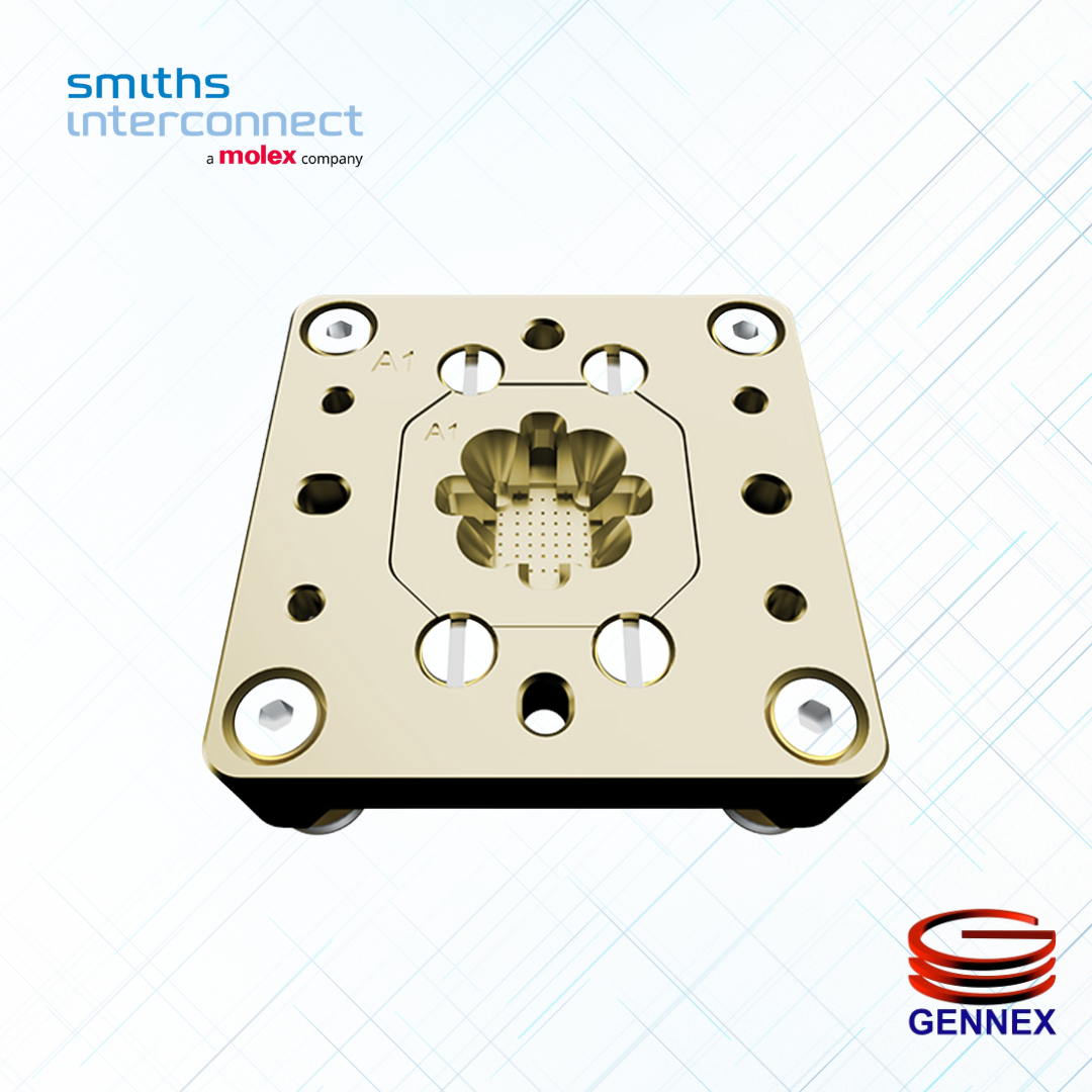
The Kepler Test Socket is engineered with advanced design and material capabilities to support reliable and high-performance semiconductor testing. The Kepler Test Sockets is designed to provide:
- Supports LGA, QFN, QFP, and other package variants
- Integrated scrub action to break through surface oxides on device pads
- Short signal path for improved electrical performance
- Tri-temperature design supporting -55 °C to +150 °C operation
- Configurable design for seamless integration into existing hardware setups
- Suitable for manual, bench, and high-volume production testing
- High-performance polyimide insulator housing for durability
- Compact footprint for space-efficient test configurations
These features make it suitable for a wide range of semiconductor test applications, from engineering validation to high-volume manufacturing.

Advantages of Using the Kepler Test Sockets
The Kepler Test Sockets delivers measurable improvements in testing performance, reliability, and efficiency. Key advantages include:
- Long contact life with durability exceeding 500,000 insertions
- Reliable and consistent electrical contact across various pad finishes
- Low and stable contact resistance for improved performance
- Excellent signal integrity for high-speed applications
- Versatility across multiple test environments and use cases
- Cost efficiency through compatibility with existing PCB footprints and hardware
- Field repairable design with easy cleaning and maintenance
- Material properties optimized for stability, including low dielectric constant and low thermal expansion
- Enables closer component placement for improved signal performance and reduced loss
Its design helps improve first-pass yield and overall production reliability, making it a strong solution for modern semiconductor testing needs.

Gennex as Reliable Support for Kepler Test Socket
Gennex provides expert support and regional service for Kepler Test Sockets solution by Smiths Interconnect, helping customers achieve optimal performance in their semiconductor testing processes. Benefits of partnering with Gennex:
- Local technical expertise and responsive support
- Assistance in selecting and integrating the right solution
- Support for installation, maintenance, and optimization
- Reliable partner for mission-critical semiconductor applications
FAQs About Kepler Test Socket
A Kepler test socket is a high-performance semiconductor test interface that uses advanced scrub contact technology, combining the benefits of cantilever contacts and spring probes to ensure stable electrical connections during IC testing. This design includes horizontal motion during contact, which helps remove surface oxides and improve reliability without damaging the PCB. Gennex can help you understand how Kepler technology fits your application — email semicon.rfq@gennexcorp.com
Kepler test sockets are designed to support a wide range of package types, including LGA, QFN, QFP, and similar peripheral IC formats, making them suitable for various semiconductor test environments. Gennex can help you verify compatibility with your device package — contact us at semicon.rfq@gennexcorp.com
Yes. Kepler sockets are engineered with a short signal path and stable contact interface, enabling strong signal integrity required for high-speed and high-frequency semiconductor testing applications. Gennex can help you select the right configuration for high-speed applications — semicon.rfq@gennexcorp.com
Yes. These sockets are built for manual testing, bench testing, and high-volume production (HVM), offering durability and consistent performance across repeated test cycles. Gennex can help you deploy Kepler sockets in your production environment — contact us at semicon.rfq@gennexcorp.com