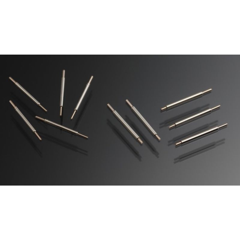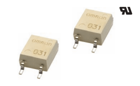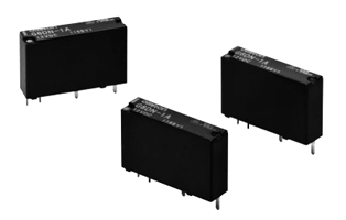

Key Features of Fine Pitch Test Solutions
Fine Pitch Test solutions are engineered to deliver consistent performance in highly demanding semiconductor testing environments. Each feature is designed to enhance accuracy, stability, and long-term operational reliability.
- High-precision probe alignment for ultra-fine pitch devices
- Excellent signal integrity for high-speed applications
- Low contact resistance for accurate measurement results
- Stable mechanical structure for repeatable testing performance
- Enhanced durability for long-term production use
- Compatible with advanced semiconductor package types
These features make the solution ideal for applications requiring high accuracy, repeatability, and stable electrical performance in semiconductor testing environments.
Need Fine Pitch Test Solutions?
Gennex can help design and support semiconductor test configurations for your application — email semicon.rfq@gennexcorp.com for project discussion.
Click HereBenefits of Fine Pitch Test:
- Improved measurement accuracy for fine pitch devices
- Reduced signal loss and contact errors
- Enhanced testing repeatability and consistency
- Increased efficiency in high-volume testing environments
- Better support for advanced semiconductor designs
- Reduced maintenance and downtime requirements
Technical Advantages of Fine Pitch Test Technology
Fine Pitch technology is built to address the challenges of ultra-miniaturized semiconductor devices, where precision and stability are critical to achieving reliable results.
- High-density contact capability
- Precision micro-scale alignment technology
- Stable electrical performance under high-frequency conditions
- Reduced probe wear for longer service life
- Enhanced thermal and mechanical stability
- Optimized for next-generation semiconductor architectures
These technical advantages makes it suitable for advanced semiconductor applications requiring exceptional precision and reliability.
Fine Pitch Test Applications
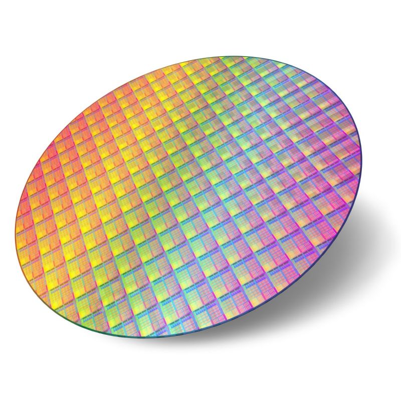
Wafer-level testing
High-density semiconductor device validation
Engineering and reliability testing
Advanced IC package testing
RF and high-speed device testing
Production-level semiconductor testing
Partner with Gennex for Fine Pitch Test Solutions
Choosing the correct Fine Pitch Test configuration is essential to ensure optimal performance and accurate results in semiconductor testing environments. Gennex team can help you identify the right solution based on your device specifications and testing requirements.
Support Services:
- Technical consultation
- Product selection guidance
- Application support
- Custom solution recommendations
- Datasheet and specification assistance
Contact our team today to learn more about Semiconductor Test solutions and find the right configuration for your semiconductor testing needs. Email semicon.rfq@gennexcorp.com for your tailored solutions.
FAQs About Fine Pitch Test
Fine pitch testing refers to the electrical testing of semiconductor devices with extremely small pad spacing, typically below 1.0 mm and down to micrometer-level geometries, where conventional probes or sockets cannot reliably make contact. It is commonly used for advanced ICs, high-density packages, and miniaturized electronic components. Gennex can help evaluate and support your fine pitch test requirements for semiconductor production — email semicon.rfq@gennexcorp.com for technical assistance.
Fine pitch test systems are commonly used for BGA, QFN, LGA, WLCSP, flip-chip devices, high-density ASICs, RF ICs, and advanced semiconductor packages used in AI, automotive, and telecommunications applications. These devices typically feature tight pad spacing that requires specialized probing solutions. Gennex can help match your device requirements with the correct fine pitch test configuration — email semicon.rfq@gennexcorp.com for application support.
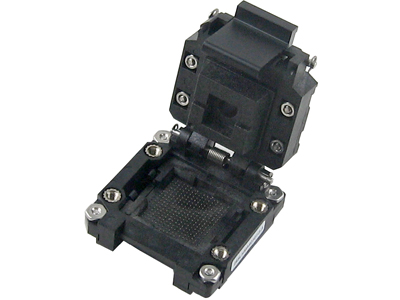
Fine pitch testing typically uses precision probe cards, spring contact probes, micro-contact interfaces, and high-density test sockets designed for tight pitch geometries. These systems are integrated into wafer test, final test, and reliability test setups depending on the application. Gennex can help you select the right fine pitch test technology for your semiconductor workflow — email semicon.rfq@gennexcorp.com for consultation.
Selecting the correct solution depends on pad pitch, device type, electrical requirements, operating temperature, test frequency, and production volume. A proper evaluation ensures better yield, reduced downtime, and improved long-term reliability. Gennex can help you choose the right fine pitch test solution based on your semiconductor device specifications — email semicon.rfq@gennexcorp.com for expert assistance.
Yes, fine pitch test solutions can be customized to match specific semiconductor device layouts, pad geometries, mechanical constraints, and electrical requirements. Customization is often necessary for advanced nodes and next-generation IC packaging. Gennex can help design and support customized fine pitch test configurations for your application — email semicon.rfq@gennexcorp.com for project discussion.
Standard probing is used for larger pad geometries with wider spacing, while fine pitch probing is specifically designed for very small pad pitches where standard probes cannot maintain stable or accurate contact. Fine pitch systems require higher precision mechanical alignment and improved electrical performance. Gennex can help determine whether your application requires fine pitch or standard probing solutions — email semicon.rfq@gennexcorp.com for evaluation support.