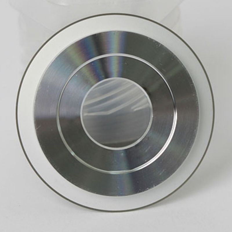
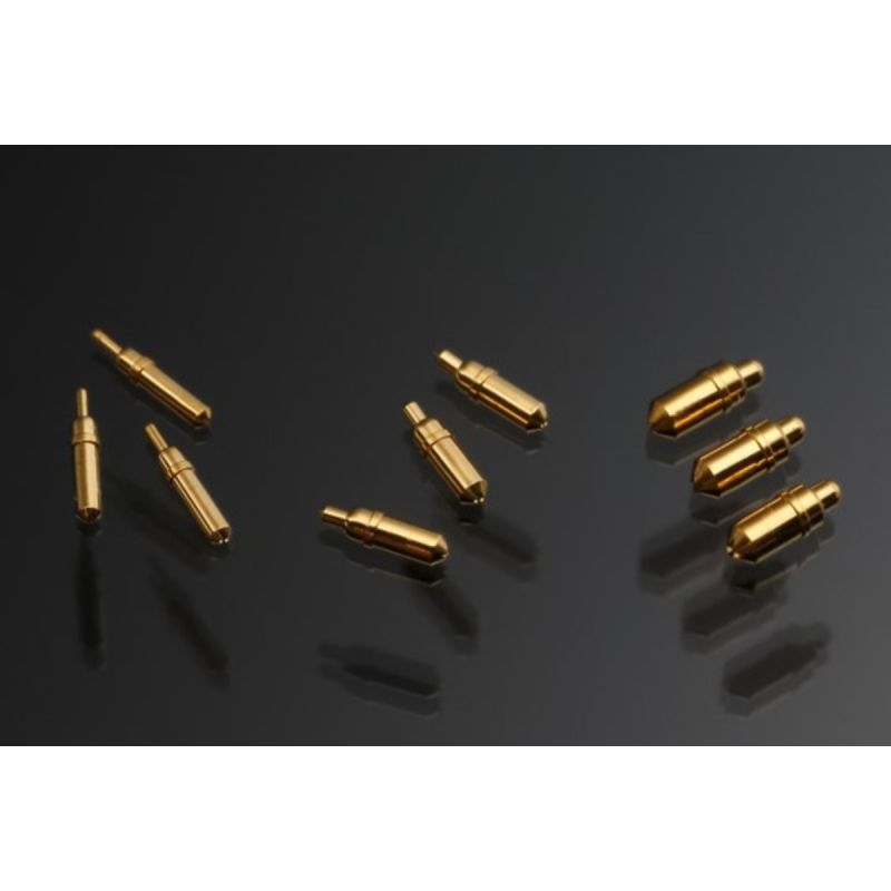
Key Features of High Frequency Test Solutions
High Frequency Test solutions are engineered to deliver stable and accurate signal performance in semiconductor environments where high-speed electrical characteristics must be preserved.
- Optimized design for RF and microwave testing
- Low insertion loss for improved signal clarity
- High signal integrity across frequency ranges
- Stable impedance matching for accurate measurements
- Reduced electromagnetic interference (EMI)
- Durable structure for repeated testing cycles
These features makes it solutions ideal for environments requiring precise signal control and consistent high-speed performance.
Need A High Frequency Test Solutions?
Contact our team today to discuss your requirements and find the right solution for your operation.
Key Benefits:
- Improved signal accuracy at high frequencies
- Reduced transmission loss and distortion
- Enhanced measurement repeatability
- Better RF device characterization
- Increased testing reliability for high-speed systems
- Improved efficiency in RF validation processes
Technical Advantages of High Frequency Test Technology
High Frequency Test technology is designed to overcome the challenges of signal degradation, impedance mismatch, and noise interference in high-speed semiconductor testing environments.
- Precision impedance control design
- High-frequency optimized signal paths
- Reduced parasitic effects for cleaner signals
- Stable performance in RF environments
- Low-loss transmission architecture
- Suitable for next-generation communication devices
These technical advantages ensure accurate and stable performance in demanding high-frequency semiconductor applications.
High Frequency Test Applications
RF semiconductor testing
High-speed IC testing
Wafer-level RF testing
Microwave device validation
5G and communication chip testing
Advanced electronic component evaluation
Partner with Gennex for High Frequency Test Solutions
Selecting the correct High Frequency Test configuration is essential for achieving accurate and stable RF and high-speed measurement results. Gennex team can help you identify the right solution based on your application requirements.
Support Services:
- Technical consultation
- Product selection assistance
- RF application support
- Custom configuration recommendations
- Datasheet and specification guidance
Contact us today to learn more about High Frequency Test solutions and find the right configuration for your semiconductor testing needs. Email semicon.rfq@gennexcorp.com for your tailored solutions.
FAQs About High Frequency Test
High frequency testing refers to the electrical evaluation of semiconductor devices operating at RF, microwave, and millimeter-wave frequencies to verify signal integrity, insertion loss, return loss, and overall device performance under fast-switching conditions. It is widely used in RF IC validation, high-speed digital testing, and advanced communication device characterization. Gennex can help support your high frequency semiconductor testing requirements with optimized solutions — email semicon.rfq@gennexcorp.com for technical assistance.
High frequency testing typically covers RF (megahertz range), microwave (gigahertz range), and millimeter-wave applications that can extend well beyond 10 GHz depending on device requirements. These ranges are used for advanced wireless, automotive radar, and high-speed digital systems. Gennex can help define the correct frequency range and testing setup for your semiconductor application — email semicon.rfq@gennexcorp.com for guidance.
High frequency test solutions are used for RF transceivers, 5G chips, Wi-Fi/Bluetooth ICs, radar sensors, high-speed SerDes devices, and mixed-signal integrated circuits used in communication and automotive systems. These devices require precise signal transmission and low-loss contact interfaces. Gennex can help match your device requirements with the right high frequency test solution — email semicon.rfq@gennexcorp.com for application support.
High frequency testing typically uses RF probe cards, precision test sockets, coaxial interfaces, vector network analyzers (VNA), and automated test equipment (ATE) designed for GHz-level measurement accuracy. These systems ensure stable and repeatable RF characterization. Gennex can help provide compatible high frequency test solutions for your semiconductor setup — email semicon.rfq@gennexcorp.com for support.
Probe and socket design directly impact signal loss, reflection, and bandwidth capability. Poor mechanical alignment or long signal paths can introduce parasitic effects that degrade RF measurement accuracy. Advanced designs minimize these effects to maintain stable high-frequency performance. Gennex can help improve your probe and socket design performance for high frequency applications — email semicon.rfq@gennexcorp.com for assistance.
Low frequency testing focuses on basic electrical parameters like continuity and DC resistance, while high frequency testing evaluates RF behavior, signal propagation, and dynamic performance under fast switching conditions. High frequency testing requires much stricter control of impedance and parasitic effects. Gennex can help determine the correct test strategy for your semiconductor requirements — email semicon.rfq@gennexcorp.com for evaluation support.
Choosing the right solution depends on operating frequency, device type, signal integrity requirements, package geometry, and test environment constraints. Proper selection ensures accurate RF characterization and long-term measurement stability. Gennex can help evaluate your requirements and recommend the most suitable high frequency test solution — email semicon.rfq@gennexcorp.com for expert guidance.